- 您现在的位置:买卖IC网 > Sheet目录320 > DK-DEV-5AGXB3N/ES (Altera)ARRIA V DEVELOPMENT KIT
AV-51001
2013.12.26
Clock Networks and PLL Clock Sources
21
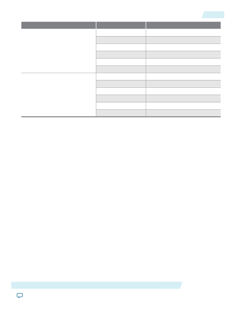
Memory Block
M20K
M10K
Depth (bits)
512
1K
2K
4K
8K
16K
256
512
1K
2K
4K
8K
Programmable Width
x40
x20
x10
x5
x2
x1
x40 or x32
x20 or x16
x10 or x8
x5 or x4
x2
x1
Clock Networks and PLL Clock Sources
Arria V devices have 16 global clock networks capable of up to 650 MHz operation. The clock network
architecture is based on Altera's global, quadrant, and peripheral clock structure. This clock structure is
supported by dedicated clock input pins and fractional PLLs.
Note: To reduce power consumption, the Quartus II software identifies all unused sections of the clock
network and powers them down.
PLL Features
The PLLs in the Arria V devices support the following features:
?
?
?
?
?
?
?
?
?
?
Frequency synthesis
On-chip clock deskew
Jitter attenuation
Counter reconfiguration
Programmable output clock duty cycles
PLL cascading
Reference clock switchover
Programmable bandwidth
Dynamic phase shift
Zero delay buffers
Fractional PLL
In addition to integer PLLs, the Arria V devices use a fractional PLL architecture. The devices have up to 16
PLLs, each with 18 output counters. One fractional PLL can use up to 18 output counters and two adjacent
Arria V Device Overview
Send Feedback
Altera Corporation
发布紧急采购,3分钟左右您将得到回复。
相关PDF资料
DK-DEV-5M570ZN
KIT DEV MAX V 5M570Z
DK-DEV-5SGXEA7N
KIT DEV STRATIX V FPGA 5SGXEA7
DK-DSP-2S180N
DSP PRO KIT W/SII EP2S180N
DK-DSP-3C120N
KIT DEV DSP CYCLONE III EDITION
DK-K7-CONN-CES-G
KINTEX-7 FPGA CONNECTIVITY KIT
DK-K7-EMBD-CES-G-J
KINTEX-7 FPGA EMBEDDED KIT JAPAN
DK-MAXII-1270N
KIT DEV MAXII W/EPM 1270N
DK-N2EVAL-3C25N
KIT DEV NIOS II CYCLONE III ED.
相关代理商/技术参数
DK-DEV-5ASTD5N
功能描述:KIT DEV ARRIA V FPGA 制造商:altera 系列:Arria V ST 零件状态:在售 类型:FPGA 配套使用产品/相关产品:Arria? V ST 内容:板 标准包装:1
DK-DEV-5CEA7N
功能描述:可编程逻辑 IC 开发工具 FPGA Development Kit For 5CEFA7F31C7N
RoHS:否 制造商:Altera Corporation 产品:Development Kits 类型:FPGA 工具用于评估:5CEFA7F3 接口类型: 工作电源电压:
DK-DEV-5CEA7N/P
制造商:Altera Corporation 功能描述:Cyclone VE Devkit Promotional 制造商:Altera 功能描述:Cyclone VE Devkit Promotional
DK-DEV-5CEA7NES
功能描述:可编程逻辑 IC 开发工具 FPGA Development Kit For 5CEFA7F3
RoHS:否 制造商:Altera Corporation 产品:Development Kits 类型:FPGA 工具用于评估:5CEFA7F3 接口类型: 工作电源电压:
DK-DEV-5CEA7NESP
制造商:Altera Corporation 功能描述:KIT DEVELOPMENT CYCLONE V E
DK-DEV-5CEA7NP
制造商:Altera Corporation 功能描述:Cyclone VE Devkit Promotional 制造商:Altera 功能描述:Cyclone VE Devkit Promotional
DK-DEV-5CGTD9N
功能描述:可编程逻辑 IC 开发工具 FPGA Development Kit For 5CGTFD9E5F35
RoHS:否 制造商:Altera Corporation 产品:Development Kits 类型:FPGA 工具用于评估:5CEFA7F3 接口类型: 工作电源电压:
DK-DEV-5CGXC7NES
功能描述:可编程逻辑 IC 开发工具 FPGA Development Kit For 5CGXFC7D6F31C7N
RoHS:否 制造商:Altera Corporation 产品:Development Kits 类型:FPGA 工具用于评估:5CEFA7F3 接口类型: 工作电源电压:
